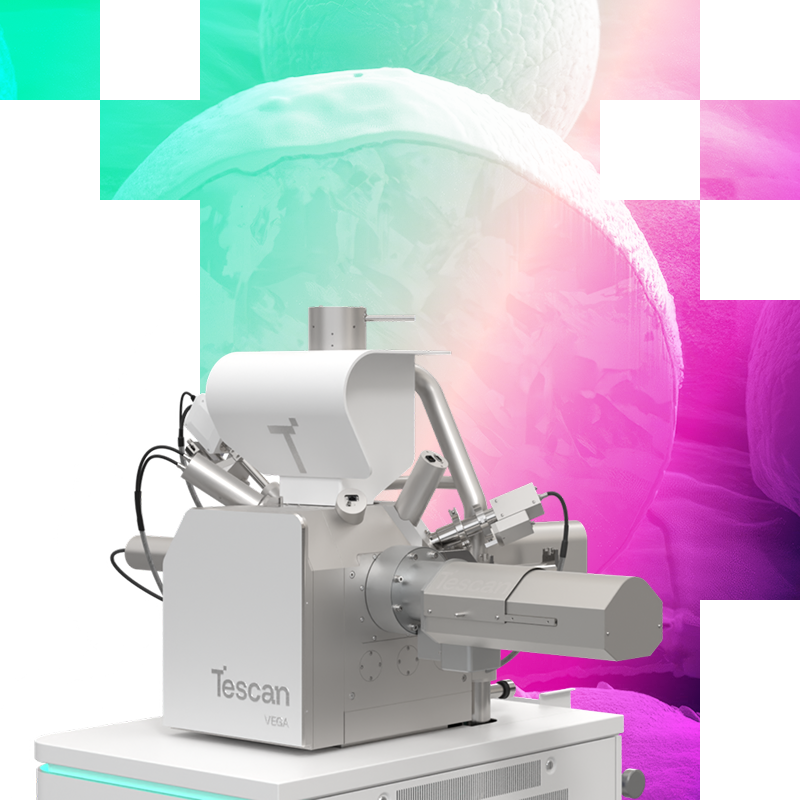
Unlike light microscopes that use visible light, an SEM fires focused electrons at a sample inside a vacuum chamber. The interaction between electrons and the sample surface generates signals that reveal fine topography, texture, and elemental composition down to the nanometer scale.
Authorities in our business will tell in no uncertain terms that Lorem Ipsum is that huge, huge no no to forswear forever. Not so fast, I'd say, there are some redeeming factors in favor of greeking text, as its use is merely the symptom of a worse problem to take into consideration.
Product care
Anyway, you still use Lorem Ipsum and rightly so, as it will always have a place in the web workers toolbox, as things happen, not always the way you like it, not always in the preferred order.
Description
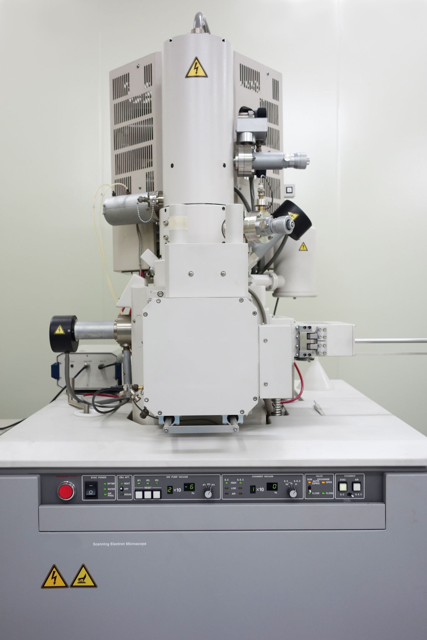
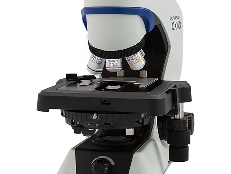
A Scanning Electron Microscope (SEM) is one of the most versatile and powerful analytical tools used in modern science, engineering, and manufacturing. Unlike conventional optical (light) microscopes that rely on photons and glass lenses, an SEM uses a focused beam of high-energy electrons to map a sample’s surface in extreme detail, producing three-dimensional topographical images down to the nanoscale.
How It Works: The Core Mechanism
Emission: An electron gun at the top of the column generates a stream of high-energy electrons (typically 0.2 keV to 30 keV).
Focusing: Electromagnetic lenses condense and focus the electron stream into a tight beam, controlling its diameter and intensity.
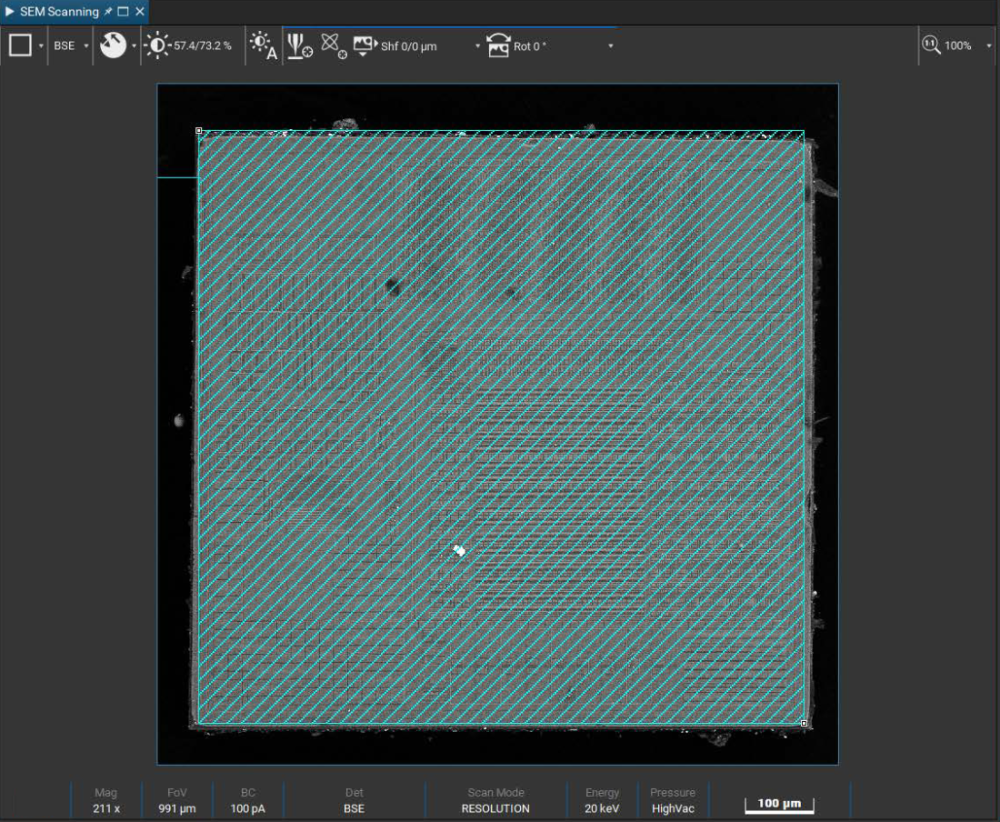
Scanning (Rastering): Scanning coils deflect the beam back and forth across the sample in a grid pattern (raster scan).
Signal Generation & Detection: When the primary electrons hit the sample surface, they penetrate a shallow region called the interaction volume and produce secondary signals.
Image Construction: Specialized detectors map the signal intensity at each point in the scan to build a high-resolution, monochrome image on a monitor.
Internal Components & Architecture
Electron Gun: The source of electrons. Common types include:
Tungsten Hairpin Filament: Traditional, cost-effective, operates at high temperatures.
Field Emission Gun (FEG): Emits a sharper, higher-brightness beam for sub-nanometer resolution.
Vacuum System: The entire column and chamber operate under high vacuum ($10^{-3}$ to $10^{-7}$ Pa). Air molecules would scatter electrons and burn out the electron gun filament if present.
Electromagnetic Lenses:
Condenser Lenses: Control the size (diameter) of the electron beam.
Objective Lens: Focuses the beam onto the sample surface.
Scanning Coils: Move the electron beam back and forth in a raster pattern across the selected area.
Sample Stage: Holds the specimen inside the vacuum chamber. High-precision motorized stages move in 5 axes ($X, Y, Z$, tilt, and rotation).
Signal Types & Detectors
When the primary electron beam strikes the sample, it generates distinct signals used for different analyses:
Signal Type
Detector
Primary Information
Secondary Electrons (SE)
Everhart-Thornley / In-Lens
Surface Topography: Low-energy electrons emitted near the surface reveal fine shape, texture, and 3D detail.
Backscattered Electrons (BSE)
Solid-State BSE Detector
Compositional Contrast: High-energy electrons reflected back by atomic nuclei; heavier elements (higher $Z$) appear brighter.
Characteristic X-rays
EDS / EDX Spectrometer
Elemental Analysis: Measures the energy of emitted X-rays to identify and quantify the chemical elements present.
Cathodoluminescence (CL)
Optical CL Detector
Luminescent Properties: Captures light emitted by semiconductors, minerals, or ceramics under electron beam exposure.







Reviews
Clear filtersThere are no reviews yet.